CPUs
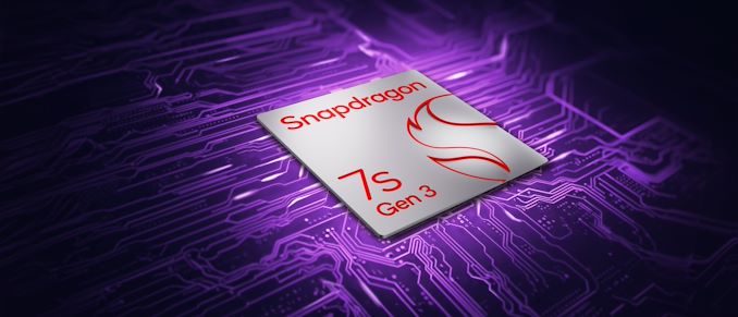
Qualcomm this morning is taking the wraps off of a new smartphone SoC for the mid-range market, the Snapdragon 7s Gen 3. The second of Qualcomm’s down-market ‘S’ tier Snapdragon 7 parts, the 7s series is functionally the entry-level tier for the Snapdragon 7 family – and really, most Qualcomm-powered handsets in North America. With three tiers of Snapdragon 7 chips, the 7s can easily be lost in the noise that comes with more powerful chips. But the latest iteration of the 7s is a bit more interesting than usual, as rather than reusing an existing die, Qualcomm has seemingly minted a whole new die for this part. As a result, the company has upgraded the 7s family to use Arm’s current Armv9 CPU cores...
Intel Sells Its Arm Shares, Reduces Stakes in Other Companies
Intel has divested its entire stake in Arm Holdings during the second quarter, raising approximately $147 million. Alongside this, Intel sold its stake in cybersecurity firm ZeroFox and reduced...
12 by Anton Shilov on 8/14/2024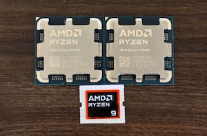
The AMD Ryzen 9 9950X and Ryzen 9 9900X Review: Flagship Zen 5 Soars - and Stalls
Earlier this month, AMD launched the first two desktop CPUs using their latest Zen 5 microarchitecture: the Ryzen 7 9700X and the Ryzen 5 9600X. As part of the...
123 by Gavin Bonshor on 8/14/2024
Intel Publishes First Microcode Update for Raptor Lake Stability Issue, BIOSes Going Out Now
Following Intel’s run of financial woes and Raptor Lake chip stability issues, the company could use some good news on a Friday. And this week they’re delivering just that...
30 by Ryan Smith on 8/9/2024
Intel Postpones Innovation 2024 Event, Cites Poor Finances
As Intel looks to streamline its business operations and get back to profitability in the face of weak revenues and other business struggles, nothing is off the table as...
15 by Ryan Smith on 8/8/2024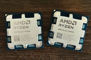
The AMD Ryzen 7 9700X and Ryzen 5 9600X Review: Zen 5 is Alive
Last month, AMD launched their first processors using the Zen 5 microarchitecture for the mobile market via their Ryzen AI 300 series. Typically, with AMD Ryzen launches, we usually...
70 by Gavin Bonshor on 8/7/2024
Intel 18A Status Update: First Chips Booting, First External Customer Tape-Out in H1’25
Following Intel’s painful Q2 earnings call and the announcement of their 2025 cost reduction plan last week, it has become increasingly evident that Intel’s future is in the hands...
14 by Ryan Smith on 8/6/2024
Update: Intel Extends 13th & 14th Gen Core Retail CPU Warranties By 2 Years In Response to Chip Instability Issues
Update 08/06: Intel published an additional note on Monday, confirming which SKUs are covered by the program. The full list of SKUs has been added to the article below...
19 by Ryan Smith on 8/6/2024
Update: Intel Accelerated Ireland EUV Fab Ramp-Up as Meteor Lake Chips Were In Short Supply
Update 08/02: Patrick Moorhead has published a further tweet, clarifying that "Pat [Gelsinger] didn’t tell me l that there were yield issues. This was *my* interpretation." The text of...
28 by Ryan Smith on 8/1/2024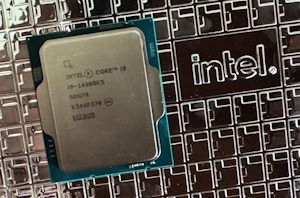
Intel Bleeds Red, Plans 15% Workforce Layoff and $10B Cuts For 2025
Amidst the backdrop of a weak quarterly earnings report that saw Intel lose money for the second quarter in a row, Intel today has announced that the company will...
68 by Ryan Smith on 8/1/2024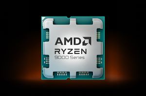
Best Buy Briefly Lists AMD's Ryzen 9000 CPUs: From $279 to $599
Although AMD delayed launch of its Ryzen 9000-series processors based on the Zen 5 microarchitecture from July 31, to early and mid-August, the company's partner (and major US retailer...
9 by Anton Shilov on 7/31/2024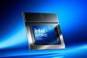
Intel to Launch "Lunar Lake" Core Ultra Chips on September 3rd
Intel’s next-generation Core Ultra laptop chips finally have a launch date: September 3rd. Codenamed Lunar Lake, Intel has been touting the chips for nearly a year now. Most recently, Intel...
17 by Ryan Smith on 7/31/2024
The AMD Ryzen AI 9 HX 370 Review: Unleashing Zen 5 and RDNA 3.5 Into Notebooks
During the opening keynote delivered by AMD CEO Dr. Lisa Su at Computex 2024, AMD finally lifted the lid on their highly-anticipated Zen 5 microarchitecture. The backbone for the...
72 by Gavin Bonshor on 7/28/2024_carousel.jpg)
AMD Delays Ryzen 9000 Launch 1 to 2 Weeks Due to Chip Quality Issues
AMD sends word this afternoon that the company is delaying the launch of their Ryzen 9000 series desktop processors. The first Zen 5 architecture-based desktop chips were slated to...
36 by Ryan Smith on 7/24/2024
Intel Addresses Desktop Raptor Lake Instability Issues: Faults Excessive Voltage from Microcode, Fix Coming in August
In what started last year as a handful of reports about instability with Intel's Raptor Lake desktop chips has, over the last several months, grown into a much larger...
49 by Ryan Smith on 7/22/2024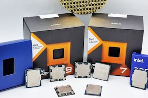
Best CPUs for Gaming: July 2024
As the second quarter of 2024 is soon set to unfold, there are many things to be excited about, especially as Computex 2024 has been and gone. We now...
11 by Gavin Bonshor on 7/17/2024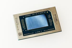
The AMD Zen 5 Microarchitecture: Powering Ryzen AI 300 Series For Mobile and Ryzen 9000 for Desktop
Back at Computex 2024, AMD unveiled their highly anticipated Zen 5 CPU microarchitecture during AMD CEO Dr. Lisa Su's opening keynote. AMD announced not one but two new client...
43 by Gavin Bonshor on 7/15/2024
Troubled AI Processor Developer Graphcore Finds a Buyer: SoftBank
After months of searching for a buyer, troubled U.K.-based AI processor designer Graphcore said on Friday that it has been acquired by SoftBank. The company will operate as a...
7 by Anton Shilov on 7/12/2024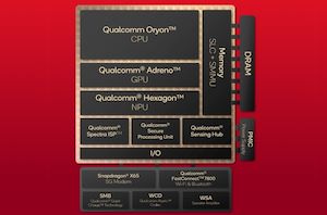
The Qualcomm Snapdragon X Architecture Deep Dive: Getting To Know Oryon and Adreno X1
The curtains are drawn and it’s almost showtime for Qualcomm and its Snapdragon X SoC team. After first detailing the SoC nearly 8 months ago at the company’s most...
52 by Ryan Smith on 6/13/2024
Report: MediaTek Working on Arm-Based Processor for Windows PCs
As Qualcomm's exclusivity for Arm-powered processors for Windows PCs is reportedly coming to its end, other chipmakers are getting ready to offer their Arm-based system-on-chips for Windows computers. And...
8 by Anton Shilov on 6/12/2024


