GPUs

AMD has made itself quite a reputation with its bundling campaigns over the years, and every new season we can be sure that the company will be giving away free games with the purchase of its hardware. This summer will certainly not be exception as AMD will be bundling Warhammer 40,000: Space Marine 2 and Unknown 9: Awakening titles with its Ryzen 7000 CPUs and Radeon RX 7000 video cards. The latest bundle offer essentially covers all of AMD's existing mid-range and high-end consumer desktop products, sans the to-be-launched Ryzen 9000 series. That includes not only AMD's desktop parts, such as the Ryzen 9 7800X3D, but also virtually their entire stack of Radeon RX 7000 video cards, right on down to the 7600 XT. AMD's laptop...
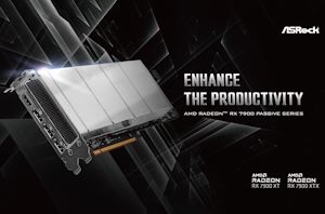
ASRock Launches Passively Cooled Radeon RX 7900 XTX & XT Cards for Servers
As sales of GPU-based AI accelerators remain as strong as ever, the immense demand for these cards has led to some server builders going off the beaten path in...
8 by Anton Shilov on 7/26/2024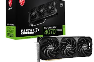
NVIDIA's AD102 GPU Pops Up in MSI GeForce RTX 4070 Ti Super Cards
As GPU families enter the later part of their lifecycles, we often see chip manufacturers start to offload stockpiles of salvaged chips that, for one reason or another, didn't...
10 by Anton Shilov on 6/26/2024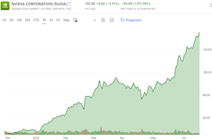
NVIDIA Closes Above $135, Becomes World’s Most Valuable Company
Thanks to the success of the burgeoning market for AI accelerators, NVIDIA has been on a tear this year. And the only place that’s even more apparent than the...
17 by Ryan Smith on 6/18/2024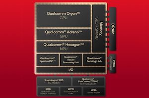
The Qualcomm Snapdragon X Architecture Deep Dive: Getting To Know Oryon and Adreno X1
The curtains are drawn and it’s almost showtime for Qualcomm and its Snapdragon X SoC team. After first detailing the SoC nearly 8 months ago at the company’s most...
52 by Ryan Smith on 6/13/2024
SK hynix: GDDR7 Mass Production To Start in Q4'2024
Update 06/13: SK hynix has sent a note to AnandTech clarifying that the company "plans to start mass production of GDDR7 in the fourth quarter of this year when...
2 by Anton Shilov on 6/11/2024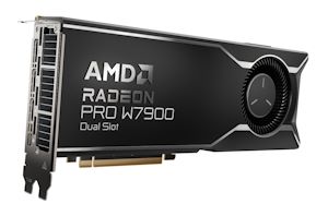
AMD Slims Down Compute With Radeon Pro W7900 Dual Slot For AI Inference
While the bulk of AMD’s Computex presentation was on CPUs and their Instinct lineup of dedicated AI accelerators, the company also has a small product refresh for the professional...
2 by Ryan Smith on 6/2/2024
AMD Plans Massive Memory Instinct MI325X for Q4'24, Lays Out Accelerator Roadmap to 2026
In a packed presentation kicking off this year’s Computex trade show, AMD CEO Dr. Lisa Su spent plenty of time focusing on the subject of AI. And while the...
3 by Ryan Smith on 6/2/2024
VESA Rolls Out DisplayHDR 1.2 Spec: Adding Color Accuracy, Black Crush, & Wide-Color Gamuts For All
VESA this morning is taking the wraps off of the next iteration of its DisplayHDR monitor certification standard, DisplayHDR 1.2. Designed to raise the bar on display quality, the...
9 by Ryan Smith on 5/7/2024
SK hynix Reports That 2025 HBM Memory Supply Has Nearly Sold Out
Demand for high-performance processors for AI training is skyrocketing, and consequently so is the demand for the components that go into these processors. So much so that SK hynix...
6 by Anton Shilov on 5/2/2024
SK Hynix and TSMC Team Up for HBM4 Development
SK hynix and TSMC announced early on Friday that they had signed a memorandum of understanding to collaborate on developing the next-generation HBM4 memory and advanced packaging technology. The...
5 by Anton Shilov on 4/19/2024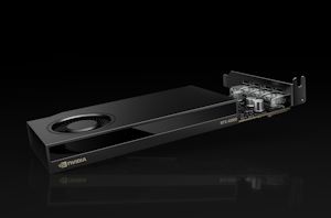
NVIDIA Intros RTX A1000 and A400: Entry-Level ProViz Cards Get Ray Tracing
With NVIDIA’s Turing architecture turning six years old this year, the company has been retiring many of the remaining Turing products from its video card lineup. And today that...
0 by Ryan Smith on 4/16/2024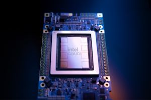
Intel Introduces Gaudi 3 AI Accelerator: Going Bigger and Aiming Higher In AI Market
Intel this morning is kicking off the second day of their Vision 2024 conference, the company’s annual closed-door business and customer-focused get-together. While Vision is not typically a hotbed...
21 by Ryan Smith on 4/9/2024
SK hynix to Build $3.87 Billion Memory Packaging Fab in the U.S. for HBM4 and Beyond
SK hynix this week announced plans to build its advanced memory packaging facility in West Lafayette, Indiana. The move can be considered as a milestone both for the memory...
7 by Anton Shilov on 4/5/2024
PCIe 7.0 Draft 0.5 Spec Available: 512 GB/s over PCIe x16 On Track For 2025
PCI-SIG this week released version 0.5 of the PCI-Express 7.0 specification to its members. This is the second draft of the spec and the final call for PCI-SIG members...
18 by Anton Shilov on 4/4/2024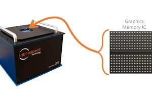
Introspect Intros GDDR7 Test System For Fast GDDR7 GPU Design Bring Up
Introspect this week introduced its M5512 GDDR7 memory test system, which is designed for testing GDDR7 memory controllers, physical interface, and GDDR7 SGRAM chips. The tool will enable memory...
0 by Anton Shilov on 3/29/2024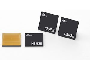
HBM Revenue Poised To Cross $10B as SK hynix Predicts First Double-Digit Revenue Share
Offering some rare insight into the scale of HBM memory sales – and on its growth in the face of unprecedented demand from AI accelerator vendors – the company...
6 by Anton Shilov on 3/28/2024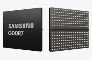
GDDR7 Approaches: Samsung Lists GDDR7 Memory Chips on Its Product Catalog
Now that JEDEC has published specification of GDDR7 memory, memory manufacturers are beginning to announce their initial products. The first out of the gate for this generation is Samsung...
18 by Anton Shilov on 3/27/2024
Micron Sells Out Entire HBM3E Supply for 2024, Most of 2025
Being the first company to ship HBM3E memory has its perks for Micron, as the company has revealed that is has managed to sell out the entire supply of...
27 by Anton Shilov on 3/22/2024
NVIDIA's GPU IP Drives into MediaTek's Dimension Auto SoCs
MediaTek this week has introduced a new lineup of Dimensity Auto Cockpit system-on-chips, covering the entire market spectrum from entry-level to premium. And while automotive chip announcements are admittedly...
6 by Anton Shilov on 3/21/2024


